HASL / ENIG / OSP FR4 mobile / cell phone pcb circuit boards 1OZ Copper Thickness
Specifications
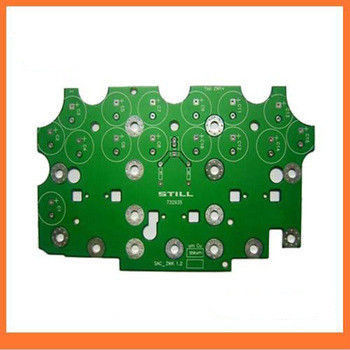
FR4 cell phone circuit boards
1.FR4 material,multi-layer pcb
2.UL,SGS,ROHS,IS09001
3.X-ray&AOI Test
FR4 cell phone circuit boards
1.HASL/ENIG/OSP finish required to meet ROHS compliant;
2.FR4 material within 0.2mm-3.2mm boards thickness;
3.Copper weight:0.5OZ,1OZ,2OZ,3OZ;
4.0.2mm min finished hole size;
5.Certificate: UL, ROHS, T/S16949;
6.Company management: ISO9001:2000;
7.Markets: Europe, America, Asia etc all over the world.
PCB manufacturing capacity
|
NO
|
Item
|
Craft Capacity
|
|
1
|
Layer
|
1-28 Layers
|
|
2
|
Base Material for PCB
|
FR4, CEM-1, TACONIC, Aluminium, High Tg Material,
High Frequence ROGERS ,
TEFLON, ARLON, Halogen-free Material
|
|
3
|
Rang of finish baords Thickness
|
0.21-7.0mm
|
|
4
|
Max size of finish board
|
900MM*900MM
|
|
5
|
Minimum Linewidth
|
3mil (0.075mm)
|
|
6
|
Minimum Line space
|
3mil (0.075mm)
|
|
7
|
Min space between pad to pad
|
3mil (0.075mm)
|
|
8
|
Minimum hole diameter
|
0.10 mm
|
|
9
|
Min bonding pad diameter
|
10mil
|
|
10
|
Max proportion of drilling hole and board thickness
|
1:12.5
|
|
11
|
Minimum linewidth of Idents
|
4mil
|
|
12
|
Min Height of Idents
|
25mil
|
|
13
|
Finishing Treatment
|
HASL (Tin-Lead Free), ENIG(Immersion Gold),
Immersion Silver , Gold Plating (Flash Gold),
OSP, etc.
|
|
14
|
Soldermask
|
Green, White, Red, Yellow, Black, Blue,
transparent photosensitive soldermask,
Strippable soldermask.
|
|
15
|
Minimun thickness of soldermask
|
10um
|
|
16
|
Color of silk-screen
|
White, Black, Yellow ect.
|
|
17
|
E-Testing
|
100% E-Testing (High Voltage Testing);
Flying Probe Testing
|
|
18
|
Other test
|
ImpedanceTesting,Resistance Testing,
Microsection etc.,
|
|
19
|
Date file format
|
GERBER FILE and DRILLING FILE,
PROTEL SERIES, PADS2000 SERIES,
Powerpcb SERIES, ODB++
|
|
20
|
Special technological requirement
|
Blind & Buried Vias and High Thickness copper
|
|
21
|
Thickness of Copper
|
0.5-14oz (18-490um)
|
PCB Superiority
1.High efficiency&Experience
We can provide one stop service.Established in 2001, with many years hard-working and constant innovation,we have
grown up into a professional PCB&PCBA manufacturer. We have our own independent research and development
department and sophisticated quality control system.
2.Quality
Our product are manufactured according to the UL/Rohs standards to insure quality assemblies from start to finish. Whether
it's a simple custom or not.Product or a complex turnkey production run, We will adhere to the highest quality standards.
3.Protecting your interests
Protecting your Intellectual Property is job one! Our staff of trained professionals are all working under a strict confidentiality
contract and treat your important documentation as they would their own.
4.Service
We can provide 24hours service for you. We pride ourselves on our ability to custom tailor programs around our customers'
needs.We take time to listen to your unique business needs and then set out to surpass them.

 ข้อความของคุณจะต้องอยู่ระหว่าง 20-3,000 ตัวอักษร!